How many patents does
National Center For Advanced Packaging Co., Ltd. have?
patents
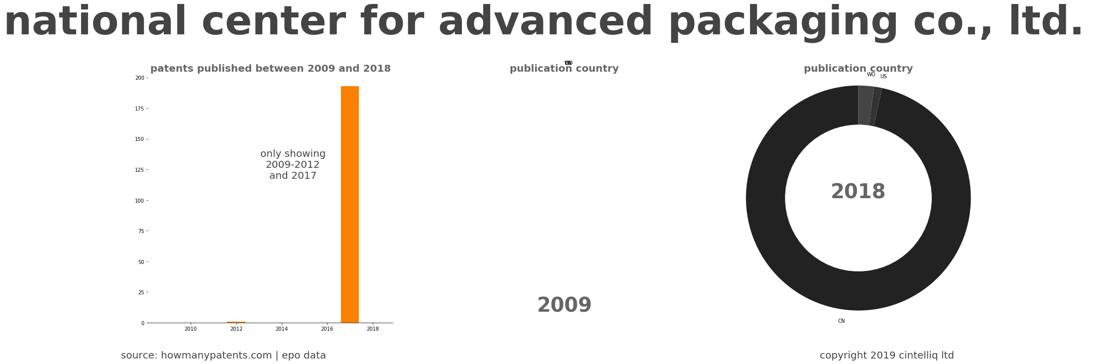
574
families
418
granted
144
applications
430
CN
558
US
12
WO
4
Buy the report
The report contains ten-year analysis with the following sections
- patent filing analysis
- worldwide filing analysis
- patent family analysis
- application analysis
- granted analysis
- classification analysis
- citation analysis
contact us for pricing
- VAT will apply to UK companies
- EU companies must supply their VAT number
Check out our sample pages |
Find companies to compare
Many companies now available
companies
12,000+
patents
42 million
patent families
23 million
Search to find companies of interest
read summary of their published patent
the following tables are just extracts from the report
the company report contains more information
National Center For Advanced Packaging Co., Ltd.
Top ten assignees appearing on patents
2009 - 2018
| national center for advanced packa… 🛈 | 248 |
| national center for advanced packa… 🛈 | 16 |
2009
National Center For Advanced Packaging Co., Ltd.
The top ten patent families are
|
Title of patent family (most common patent title) |
Family members |
Filing year |
|---|---|---|
| tsv backside reveal structure and exposing process | 5 | 2013 |
| method for flattening surface of substrate by adopting cmp in pinboard process | 4 | 2014 |
| optical communication device and assembly method thereof | 4 | 2015 |
| fan-out-type wafer level package method | 4 | 2015 |
| active optical adapter plate and optical interconnection module | 4 | 2015 |
| silicon through hole patch board wafer testing system and method | 3 | 2014 |
| heat radiation structure used for bga (ball grid array) package of high-power chip | 3 | 2014 |
| photo chip of backward scattering grating coupled packaging structure and manufacture me… 🛈 | 2 | 2015 |
| flexible-substrate-based three-dimensional packaging heat-radiation structure and prepar… 🛈 | 2 | 2015 |
| package stack heat radiating structure with recessed heat radiating plate base and manuf… 🛈 | 2 | 2015 |